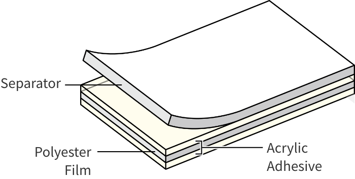
Masking tape
for semiconductor package substratese
Features
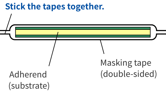
Masking tape is used as a protective tape for solder resist in the multilayer PCB manufacturing process, mainly for FC-BGA substrates.
- Prevention of oxygen inhibition of solder resist is realized.Recommended products for RESONAC's (Showa Denko) Solder Resist/SR7300 and SR7400A
- Silicone-free design to prevent repelling of ink characters
- Combines adhesion and peelability with no adhesive residue
- Good substrate flatness
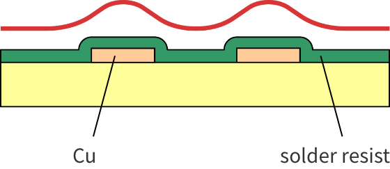
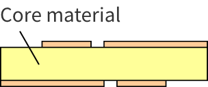
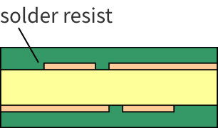
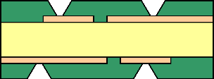
Substrate surface flatness
The use of masking tape prevents ridges of the solder resist, enabling a flat substrate surface.
Improve underfill fillability and increases yield in manufacturing multi-level substrate.
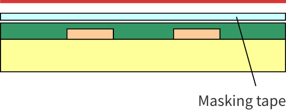
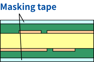
Control of contamination and oxygen inhibition
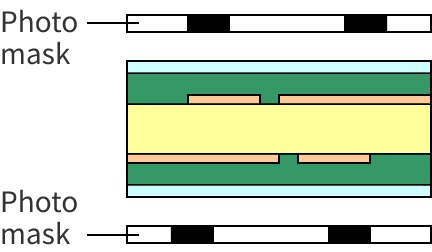
As shown in the figure below, masking tape can be applied to both sides of the substrate and sealed to prevent oxygen inhibition of the solder resist.
Rollers can be applied to remove contamination prior to developing and to prevent dust emission from substrate edges.
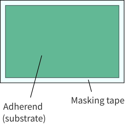
Applications
Process Image (FC-BGA Substrate Manufacturing)
line-up
| Item | Unit | #3250A | #3750 | |
|---|---|---|---|---|
| thickness | Base material | μm | 12 | 12 |
| Adhesive | μm | 2 | 8 | |
| Separator | μm | 30 | 30 | |
| Adhesive strength to SUS | N/25mm | 0.14 | 0.50 | |
| Separator peeling force | N/25mm | 0.09 | 0.20 | |
| Total Light Transmittance | % | 91.9 | 91.2 | |
| Haze | % | 4.2 | 3.7 | |
Note
Combines adhesion and peelability with no adhesive residue
ATR spectra of substrate surface
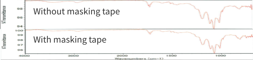
ATR spectral analysis of the surfaces of substrates with and without using masking tape shows no difference.
IR spectra of extracts from substrate surface
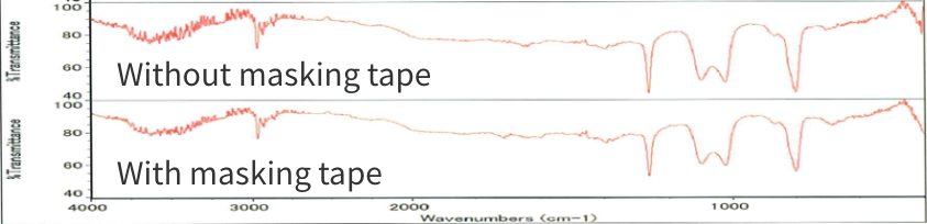
IR spectral analysis of extracts obtained from substrates with and without using masking tape shows no differences.