- Top Page
- Product Development Story
SEKISUI
Product Development
Story
 Continuing to support the evolution
of semiconductor processes with
innovative technology for
'adhesion and peeling'—
SELFA™
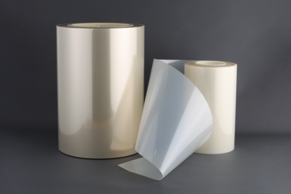
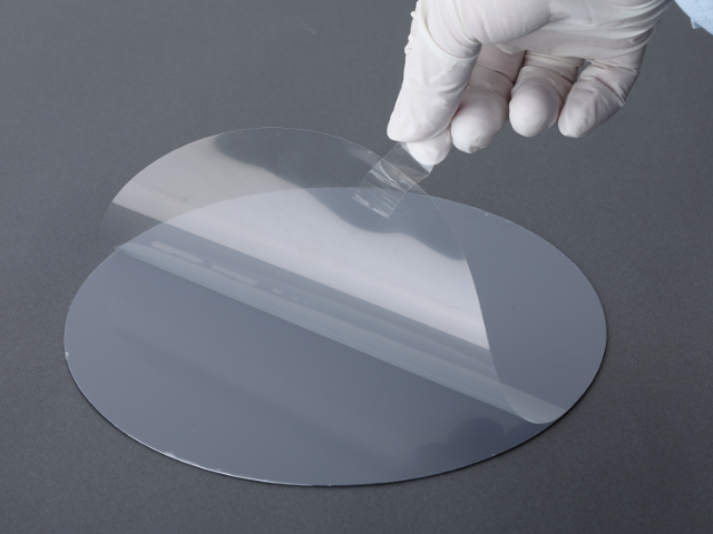
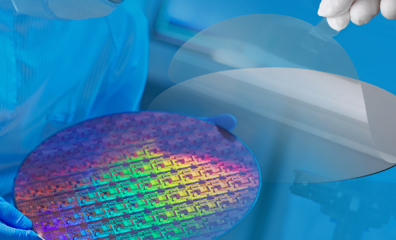
SEKISUI CHEMICAL has been engaged in the development of materials related to semiconductor wafer/chip manufacturing processes for many years. Among various products, the tape-type temporary adhesive material SELFA™, which is essential for polishing processes such as wafer lapping, has received strong support from many semiconductor manufacturers due to its unique characteristics.
The journey to product commercialization was never straightforward, and as the semiconductor processes evolve, so does our product. We asked the engineers involved with SELFA™ to share their insights on its development history and their aspirations for future product creation.


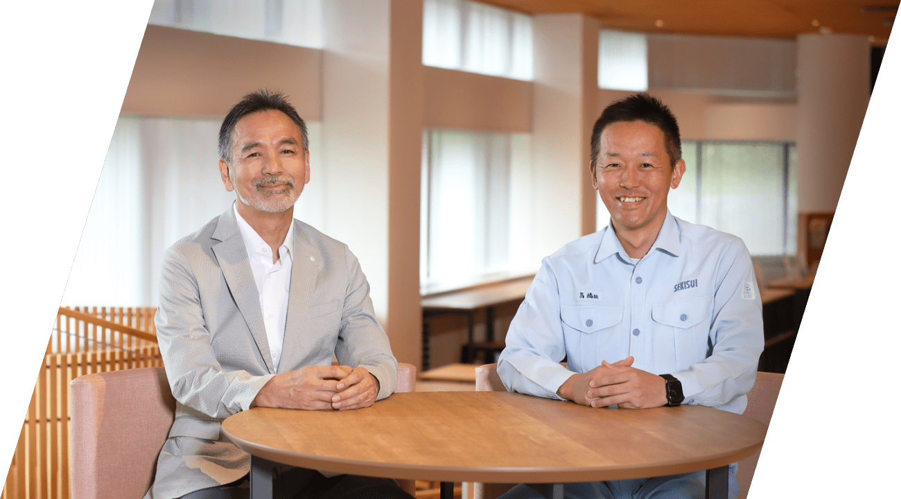
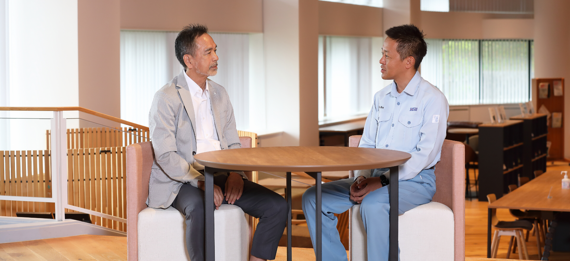
- Akira Nakasuga
- Former Director of the Research & Development Institute
(retired in 2019),
High Performance Plastics Company
Current Representative of Science Lab Ishizue

- Toshio Takahashi
- Chief Engineer, Electronics Materials Development Center
Research & Development Institute
High Performance Plastics Company
Talk 01
Challenging the Semiconductor Market
with Innovative 'Easy Peel' Technology
Can you tell us about the development history of SELFA™?
Nakasuga : As part of its growth investment, SEKISUI CHEMICAL established the "Adhesive Technology Center" in Kyoto in 1991, led by the first director who championed the slogan "Let's create a hub for cutting-edge polymer processing technology," and attracted excellent engineers. This can be considered the origin of the SELFA™ development.
Since around 1990, I have been involved in research on light-curable adhesives that led to the current "UV release technology," and in 1995, I became the head of the Adhesive Bonding Technology Center, promoting its development. By mixing light-curable materials into the adhesive and exposing it to UV light, the adhesive interface becomes easier to peel. While I was conceptualizing products based on this characteristic, another company had already commercialized a tape for temporarily fixing semiconductor wafers, which inspired SEKISUI CHEMICAL to pursue a similar direction.
We completed SELFA™ in 2002, obtained the trademark and launched it. Initially, the response from semiconductor manufacturers was weak, and it was difficult to gain adoption. The development team dwindled, and we faced a challenging period.
What was your impression of the development department when you joined?
Takahashi : When I joined in 2009, SELFA™ had already been commercialized, but to be honest, the development department wasn't very prominent within the company.
Nakasuga : The semiconductor manufacturing process requires advanced technology and equipment, and a decrease in yield rates can result in significant losses. Therefore, temporary adhesive materials used to protect wafers must ensure a high level of quality and stability. New process materials like SELFA™ often have trouble being adopted without a proven track record.
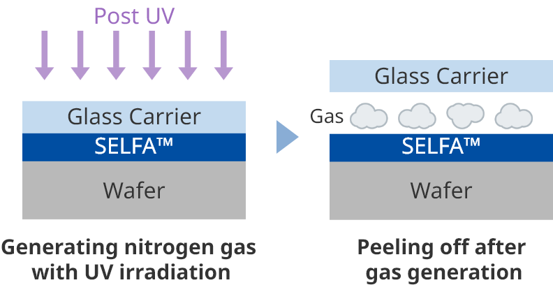
Takahashi : The biggest feature of SELFA™ is its "UV self-release" capability. The idea of concentrating gas in the gap between the tape and substrate or subject to promote peeling was unique. However, even with such a distinct advantage, entering the semiconductor market as a new player was challenging.
I've heard that even during the tough times when sales were low, you did not give up on the development and continued pushing forward. If you had given up then, SELFA™ wouldn't exist today, so I think that decision was remarkable.
What was the turning point for the significant increase in SELFA™ sales?
Nakasuga : Overseas semiconductor manufacturers had an interest in building relationships with Japanese companies that lead in materials technology, resulting in many cases where they adopted materials from Japanese manufacturers.
Given this context, SEKISUI CHEMICAL shifted its focus from domestic markets to major overseas semiconductor device manufacturers.
Around that time, major semiconductor device manufacturers were advancing new package development. In response, SELFA™ underwent continuous improvements to meet the demanding requirements. As a result, companies decided to adopt SELFA™, and sales numbers surged. It took about 15 years from the birth of the technical concept to achieve that success.
Takahashi : Today, with active sales and marketing efforts, SELFA™ has established itself in the temporary adhesive market as a "high-performance, high-end temporary adhesive tape." I believe this is a testament to the perseverance and skill development of my predecessors who were involved in its creation.
Talk 02
Going Beyond Heat Resistance Limits?
Facing Thermal Issues in Semiconductor Manufacturing
As digital devices advance and the semiconductor market continues to expand,
what is the current status of SELFA™ development?
Takahashi : Components for mobile devices are shrinking in size, as these devices keep getting thinner, lighter, and more sophisticated. In the future, semiconductor wafers will become increasingly thinner and more prone to damage, while components will also get smaller and wiring finer, making thermal management even more critical. We are progressing with product development based on the prediction that thermal management will become stricter. "UV gas release technology," which concentrates gas between the tape and the subject to lift it without stressing the device, has advantages over other methods. However, as TSV technology (3D packaging) advances and semiconductor devices become ultra-thin and multilayered, materials that can withstand even higher temperatures will be required for more efficient heat dissipation.
Mr. Takahashi, you are involved in the development of "heat resistance."
Is it possible to realize a SELFA™ that can withstand even higher temperatures?
Takahashi : We are aiming for super heat resistance that can be used at temperatures close to 300°C, but there are several significant challenges to address. For example, the UV gas-generating substances within the tape can decompose at high temperatures, and the residues generated from thermal processing are also problematic.
However, if we can achieve an innovative tape that can withstand ultra-high temperatures, it could not only replace liquid products currently used at high temperatures but also provide new options for our customers in process development.
Nakasuga : Currently, the heat resistance of SELFA™ has reached 260°C, but I believe that even higher heat resistance and easy peeling will be required in the future. If you can clear the heat resistance issues and develop products for even higher temperatures, there will be opportunities for creating new markets.
Will SELFA™ continue to evolve in the future?
Takahashi : As wafers become thinner and more fragile, I foresee that the residues and peeling force of SELFA™ during the release process may eventually become insufficient. Even if we can reduce the peeling force to half based on existing technology, if the future requirement is to reduce it to one-tenth, we won't meet our goals at all. In that case, we need to explore lower-stress methods beyond UV gas release technology, as well as continue to refine the existing technologies we've developed.
Nakasuga : SEKISUI CHEMICAL's fundamental approach is to respond to high-level requirements and to enter niche markets, and that philosophy underpins the development of SELFA™.
What do you consider important in solving various challenges?
Takahashi : Since this is not something that can be achieved overnight, it's necessary to broaden our perspective. While utilizing materials informatics and AI for efficiency is essential, we also aim to enhance efficiency by collaborating with the basic research department separately from the SELFA™ development department. Additionally, we want to explore collaboration beyond our own technologies, including partnerships with universities and academic societies, and consider combining technologies from other fields. Development methods are continuously evolving.
Nakasuga : In our time, the primary goal was to penetrate the market by developing products that other companies couldn't replicate with our own technology. So, we worked long hours, often with overtime, but it seems that's not the case anymore. The importance of anticipating future needs has grown.
Talk 03
Continuing to Support the Future of Semiconductors
through Advanced Materials Development
How do you plan to approach development in the future?
Takahashi : SEKISUI CHEMICAL believes it's essential to intentionally select high-barrier needs, such as wafers becoming very thin and challenging to peel or requiring exceptional heat resistance. The challenges we face are significant, but I see value in tackling them, and I believe it will lead to substantial demand in the future.
Nakasuga : I see. In our time, the focus was on developing technology that would allow us to engage with customers, but it seems the environment has changed.

Takahashi : We have an environment where we can develop alongside our customers. This allows us to understand potential issues that may arise in the future from the early stages and ensure effective product development.
As a materials manufacturer, SEKISUI CHEMICAL recognizes the importance of deepening its understanding of process technology, just like its customers in the semiconductor industry. Although we do not have a dedicated equipment development department, we see our ability to collaborate deeply with various equipment manufacturers as an advantage in our material development efforts.
Nakasuga : Additionally, setting high goals with a long-term perspective and approaching challenges boldly are necessary for development.
Takahashi : The contributions of accumulated technology from the past are indeed significant, but in terms of matching future needs, what's crucial is how quickly, accurately, and reliably we can develop our products. The difficulty of development has increased considerably, so there are many things we cannot do now. However, rather than stopping and listing reasons for what we cannot achieve, I believe it's essential to think about what is needed to make it possible and to keep executing that "cycle" continuously. It's a very simple process, but I think that by persistently following through, we can achieve significant breakthroughs.
What other challenges do you face?
Takahashi : Since SELFA™ is a process material, it gets discarded once its use in the customer's process is complete. It's important to reduce waste, so designing products that use environment-friendly, bio-based solvents is a significant theme. If we can create such solutions, the market will be more receptive, and I believe we should propose environmentally conscious products to semiconductor manufacturers.
Finally, what are your expectations for the development of SELFA™?
Nakasuga : It's essential to challenge themes that other manufacturers are not tackling. Innovations in materials technology take decades. Without continuous development, "innovation" cannot occur, and it's this pursuit of dreams that makes materials development exciting.
Takahashi : I completely agree. As materials manufacturers, we should actively incorporate the "cutting-edge challenges" posed by semiconductor manufacturers and work to solve them by combining material and process technologies. We will continue to create new value through our manufacturing efforts.
Nakasuga : You must develop products that shape both your customers' dreams and your own—ones that elicit the response, "This is interesting!"
Thank you for speaking with us today.
- UV Releasing Tape SELFA™
- Realizing a new semiconductor process with UV tape that combines heat resistance and easy peelability. Go to product details page
The information is current as of October 2024.