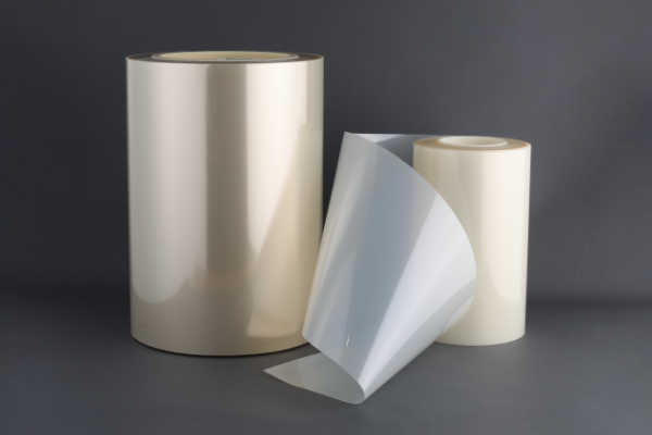
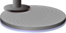
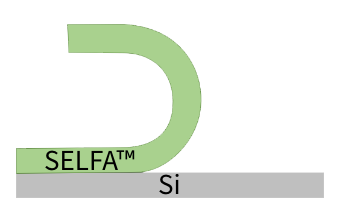
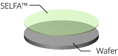
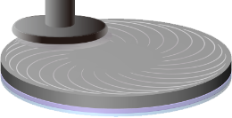
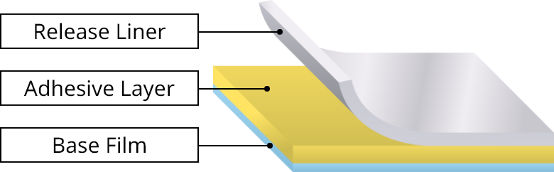
“SELFA™” , enabling new semiconductor process by high thermal resistance and debonding technology.
What is SELFA™?
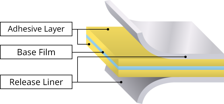
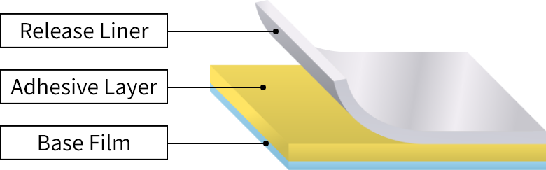
SELFA™ is a UV release tape that achieves strong adhesion and easy peeling. By UV irradiation, N2 gas is generated between the tape and the subject, nullifying adhesion strength and allowing it to be easily peeled off.
Point!
It can be easily peeled off without causing any damage to thinly polished wafers.
When is SELFA™ used?
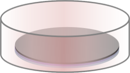
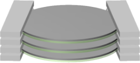
SELFA™ is mainly used in the manufacturing of semiconductor wafers and chips. Currently, we offer a lineup of three types of products for various processes such as package manufacturing, wafer support, and plating processes.
Point!
Both single-sided and double-sided types are available based on different applications.
Enables implementation of new processes such as reflow
Worried about damage to wafers
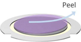
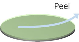
Easy Peeling
Damage-free peeling technology using gas generation
High compatibility for ultra-thin devices
Need to eliminate the residue during thermal processes
Low Residue
Residue-free using Pre UV technology
Wide process window
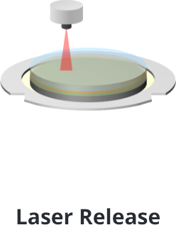
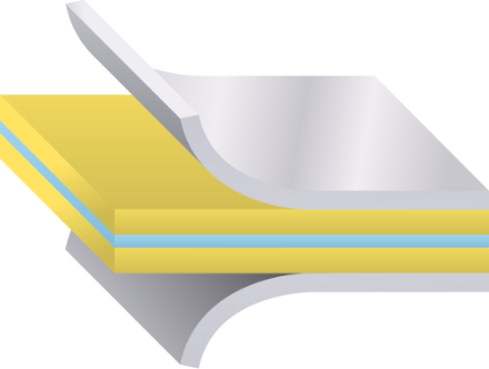
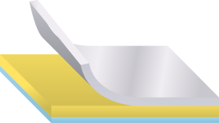
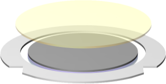
SELFA™'s Peeling-off Technology
SELFA™'s peeling-off demo video
You may find an advanced technology not found in other companies' products, enabling easy peeling-off without damaging the delicate wafer surface.
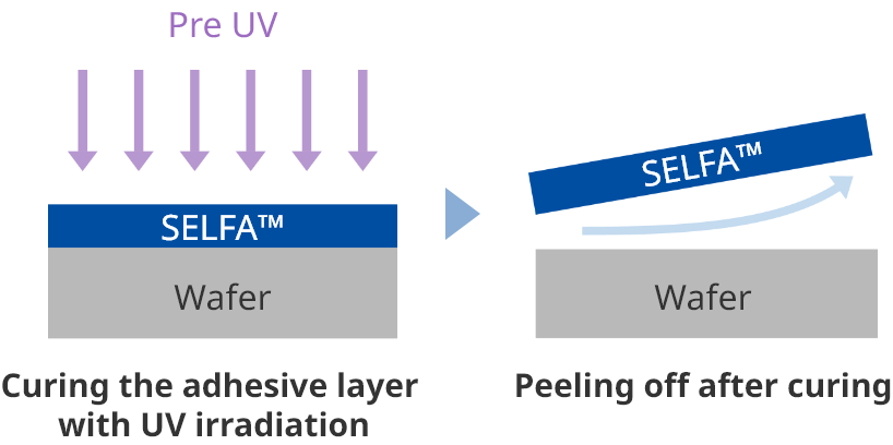
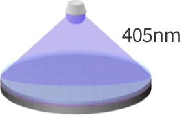
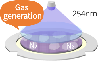
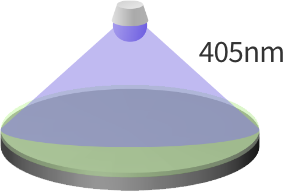
Two-step UV Irradiation
1Pre UV Curing
The adhesive strength of conventional UV tapes increases during thermal treatment and does not decrease significantly after UV exposure, making it difficult to be peeled off, leading to residue issues.
By curing the adhesive layer with Pre UV, SELFA™ significantly reduces adhesive strength which will not climb up sharply even after thermal treatment, making it much easier to be peeled off by much less force leaving much less residue.
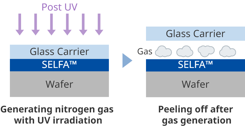
2Gas Generation
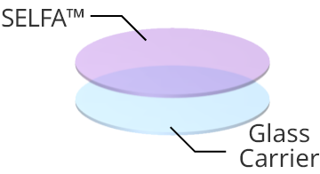
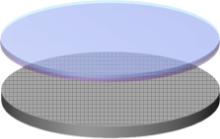
During the UV irradiation, nitrogen gas is generated between SELFA™ and the glass carrier. The gas region expands and eventually spreads across the entire surface.
After the UV irradiation, the carrier glass can be easily removed with almost no force.
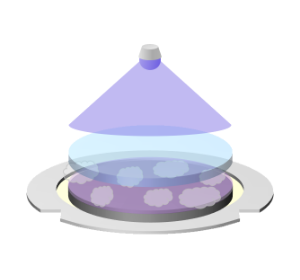
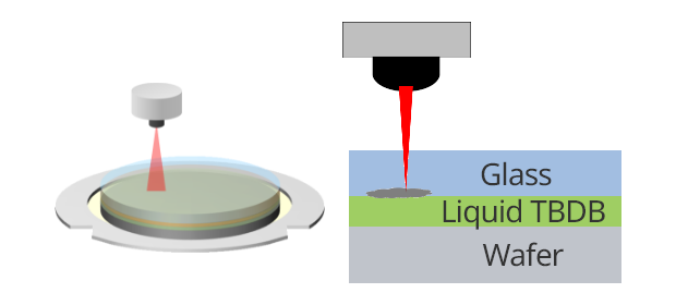
Comparison of Processes between SELFA™ and Liquid Materials
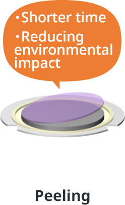
Using SELFA™ significantly shortens the Lamination and peeling processes.
Liquid Materials
SELFA™
SEKISUIProduct Development Story
Continuing to support the evolution of semiconductor processes with innovative technology for 'adhesion and peeling'— SELFA™
Former Director of the Research & Development Institute (retired in 2019),
High Performance Plastics Company
Current Representative of Science Lab Ishizue
Akira Nakasuga
Chief Engineer, Electronics Materials Development Center
Research & Development Institute
High Performance Plastics Company
Toshio Takahashi
SELFA™Lineup
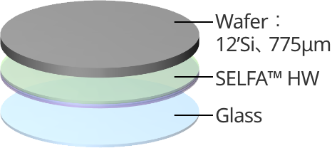
Double Sided Thermal Resistant SELFA™ HW Series
BG 〜Dicing Process
High resistance to heat and chemicals
N2 Gas-release debonding mechanism results in damage free debonding
Tape type adhesive supported glass carrier enables better handling capabilities
Using tape type adhesive to support glass carrier enables better handling capabilities.
N2 Gas-release debonding mechanism results in damage free debonding.
High resistance to heat and chemicals.
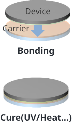
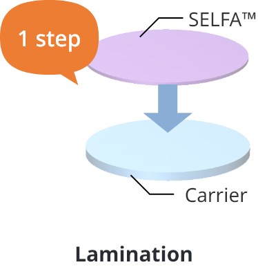
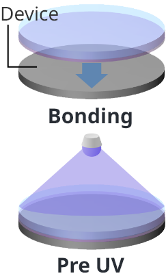
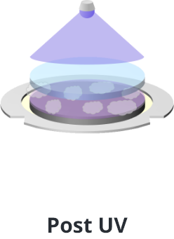
Process
Laminating
Bonding
Pre UV
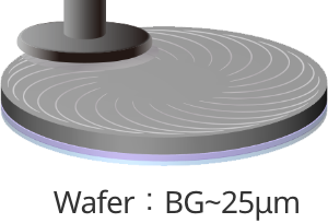
BG
Thermal Process
Dicing Tape
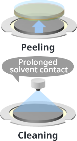
Post UV & DB
De-Taping
Evaluation results
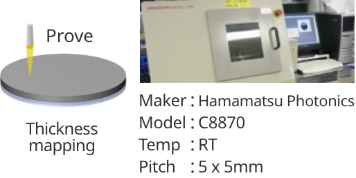
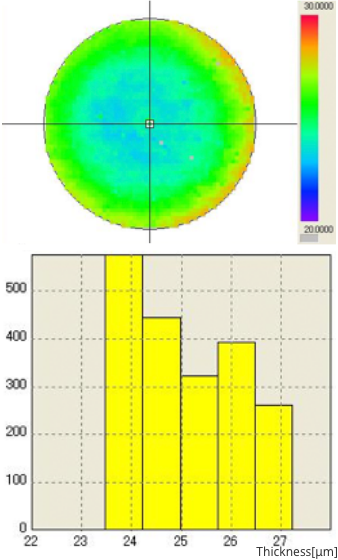
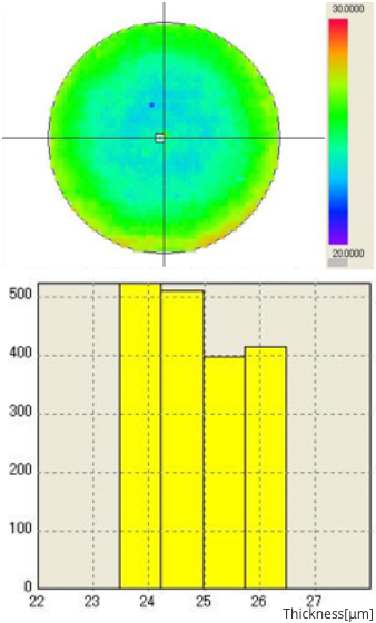
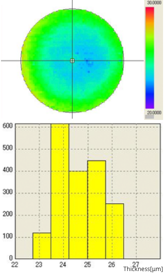
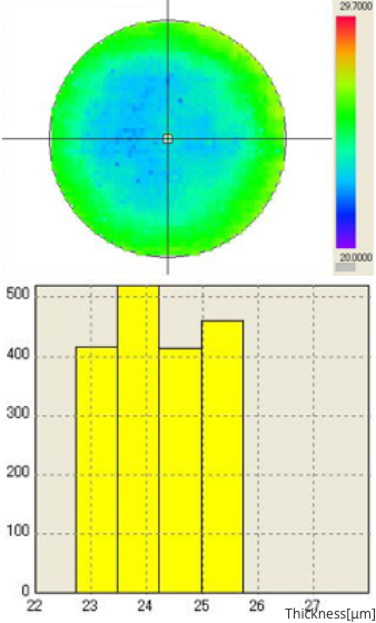
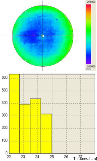
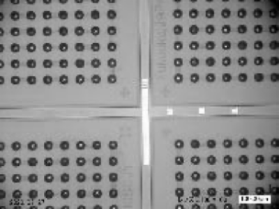
Ⅰ.Mirror Wafer TTV Evaluation after BG
Evaluation Method
TTV Mapping Result
【Average】 Thickness : 24.4μm/ TTV : 2.9μm
n=1
n=2
n=3
n=4
n=5
Thk:25.1μm TTV:3.4μm
Thk:24.5μm TTV:2.8μm
Thk:24.7μm TTV:2.9μm
Thk:24.3μm TTV:2.7μm
Thk:23.4μm TTV:2.9μm
Our unique “PreUV technology” can provide industry’s highest level TTV controllability.
<3μm@12” wafer
Ⅱ.Residue After Thermal Process<Oven and De-taping evaluation>
Point :
Thermal resistant
Equipment & Conditions
Maker: ETAC
Model: CSO-603BF
Temp: 180〜220°C
Time: 1〜2hr
Wafer & Sample
8inch Bump TEG Wafer
Results
180°C
200°C
220°C
1hr
2hr
No residue on the patterned TEG wafer after a thermal stress of 220°C 2hr.
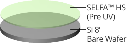
Single Sided Thermal Resistant SELFA™ HS Series
Characteristic:
Thermal Resistance
Chemical Resistance
Low Residue
Supports and protects devices during thermal processes such as reflow, CVD, and sputtering.
Process
Laminating
Pre UV
BG
Transporting
Thermal Processes
De-Taping
Thermal Resistance Evaluation (Void)
Hot Plate Evaluation
Sample
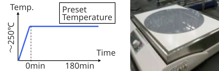
Equipment & Conditions
Maker: NINOS
Model: ND-3H
Temp: 180-250°C
Time: 30-180min
Results
Peeling-off Ability After Heating
30min
60min
120min
180min
180°C
OK
OK
OK
OK
220°C
OK
OK
OK
OK
250°C
OK
OK
OK
OK
The data shown above is measurement value, not guaranteed value.
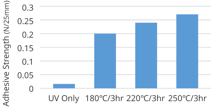
Adhesive Strength After Heating
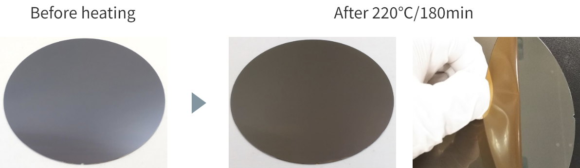
Wafer State After Heating
In hot plate evaluations, it has been confirmed that no void occurs during thermal treatment and no residue is generated during peeling, even at up to 220°C for 180 minutes.
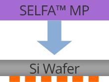
Single sided Self Release SELFA™ MP Series
Characteristic:
Easy-peeling
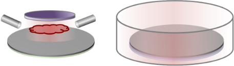
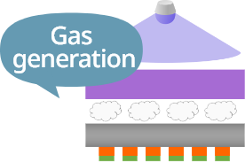
SELFA™ MP is used for protecting the backside of wafers during plating processes. UV irradiation generates gas, allowing it to be peeled off from the subject easily.
The Wafer Protection Process During Electroless Plating Treatment (Electroless Plating Method)
Tape lamination
Acid, alkali plating process
UV irradiation
After de-taping
SELFA™ MP has excellent resistance to strong acids and strong alkalis during the plating process, and after protecting the wafer, it can be peeled off with low stress.
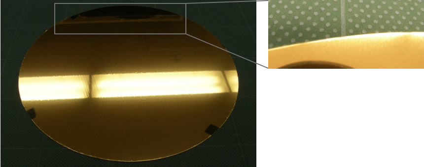
Voids and Residue Results
Point:
Easy-peeling
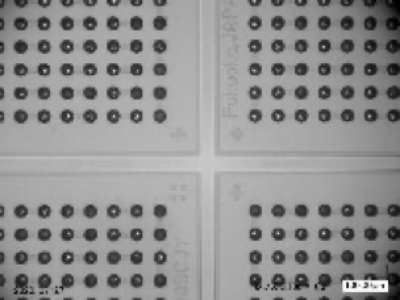
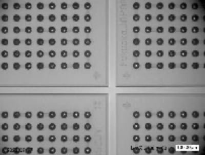
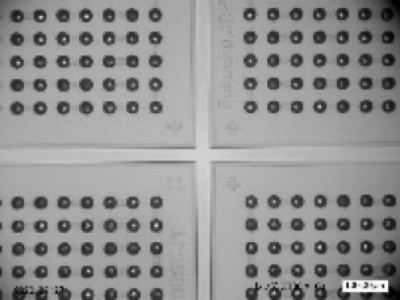
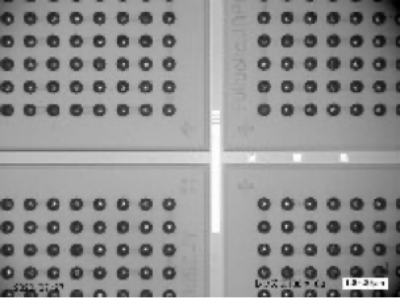
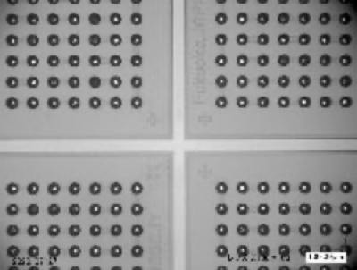
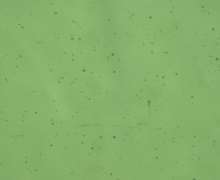
Wafer After Au Plating
No void, no edge delamination
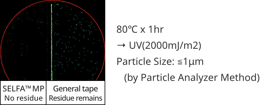
Organic Residue Inspection @8’ Wafer
No residue was observed after peeling off SELFA™ MP
Process Automation of Double-sided SELFA™
Compatible with fully automated processes, contributing to improve productivity and reduce environmental impact.
By partnering with equipment manufacturers, we can build fully automated equipment. Significant productivity improvements and reductions in environmental impact can be achieved.
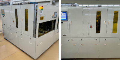
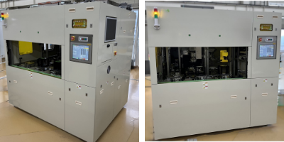
Equipment Introduction
①Wafer Bonder
Takatori Corporation WSM-200B
②Wafer Debonder
Takatori Corporation WSR-200
Reuse of Glass Carrier
By utilizing SELFA™, glass carriers can be reused more than twice much as before, also better for SDGs.
Carrier Glass Reusability
SELFA™ does not cause damage during UV irradiation, and is superior in terms of glass carriers’ recycling.
Former Director of the Research & Development Institute (retired in 2019),
High Performance Plastics Company
Current Representative of Science Lab Ishizue
Akira Nakasuga
Chief Engineer, Electronics Materials Development Center
Research & Development Institute
High Performance Plastics Company