Semiconductor Production Process
- Top Page
- Semiconductor Production Process
Production process flow related to semiconductors
The Electronics Strategy Office is running a wide material portfolio of tape/film/precise particles/sealing material. We are providing high functional products especially for the frontier needs in semiconductor industry, such as Fine L/S, high integrated design, 3D assembly, ultra thin membrane.
Wafer/chip production process
-

-
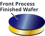
Protection Tape Lamination
High Adhesion-Easy Removable UV Tape Heat Resistant SELFA™ -

Back Grinding
-

Chemical Plating・
High Adhesion-Easy Removable UV Tape Heat Resistant SELFA™
High Temperture Treat -

Dicing Tape Lamination
-
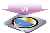
UV Irradiation・
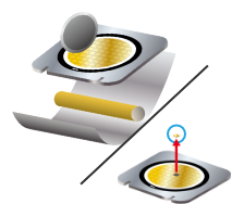
Protection Tape Removing -
-

Chip Completion
Package substrate production process
-

Copper Core Manufacture
-

BUF Stacked
Build Up Film -

Via, Dismear, Plating,
Masking tape for semiconductor package substrates
Solder Resistant Coating. -
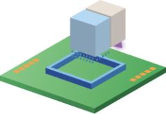
Print DAM material
High-viscosity inkjet ink
Inkjet Material -

Package Substrate Completion
1+2Assembly production process
Wafer/Chip Production Process Related Material
For various semiconductor devices such as logic, memory, and power devices, process materials that help enhance performance and yields are lined up. Our products include double-side tape optimally designed for polishing pads used in wafer planarization processes such as CMP and lapping, clean containers that deliver various chemicals used in wafer processing to wafer fabs in a clean and safe manner, and removable UV tape SELFA™ series featuring excellent heat and chemical resistance widely used for advanced packages—including fan-out and 2.5D/3D structures—and semiconductors and such.
| Material Category |
Product | Feature | |
|---|---|---|---|
| Removable UV Tape | Single-sided Heat Resistance UV Tape [SELFA™ HS] |
UV release tape that combines resistance to various semiconductor manufacturing processes with low residue. Protects device surfaces and suppresses warpage in various PKG manufacturing processes. | Product Information |
| Removable UV Tape | Double-sided Heat Resistance UV Tape [SELFA™ HW] |
UV release tape that combines resistance to various semiconductor manufacturing processes with low residue. Glass support system maintains device flatness during the process and ensures safe handling. | Product Information |
| Removable UV Tape | Single-sided Chemical-resistant Self-releasable UV Tape [SELFA™ MP] |
UV release tape that combines strong chemical resistance and low residue; UV irradiation causes gas generation, which reduces device damage and allows easy peeling. | Product Information |
| Tape | Double-faced Tape for Fixing Polishing Pads for LCD Glass Substrate, CMP, and HDD Substrate | Highly chemical-resistant tape with no adhesive residue when peeled off. Used for fixing polishing pad in the polishing process for electronic devices. Max. width 2450mm, suitable for CMP process. | Product Information |
| Container | Clean bottle | A clean bottle made from resin raw materials that have extremely low metal ion elution. The bottle is manufactured in a clean, particle-controlled environment and contributes to the stable quality of final products. The product has been used for transporting various types of high-purity chemical solutions in semiconductor and other fields. | Product Information |
Package Substrate Production Process Related Matierial
In advanced packaging, technological innovation in the aspect of materials is also required for substrates and their related areas. We contribute to the evolution of package substrates with our technologies that no other company can provide, such as Insulation Dielectric Material (build-up film) for FC-BGA featuring low transmission loss, protective film for liquid solder resist helping enhance yields and reliability of FC-BGA, and inkjet materials that allow microscopic 3D structures/patterns in several tens microns to be formed on demand.
… Sustainability Products
| Material Category |
Product | Feature | |
|---|---|---|---|
| Inkjet Materials | Pattern formation of exterior peripheries/Usage for package miniaturization [High-viscosity inkjet ink] |
Proprietary high-functionality materials, designed uniquely from adhesives to barrier rid forming materials. Freely controllable ink application shapes. Optimizing printing processes with our one-stop development. | Product Information |
| Film | Interlayer Insulating Film for Making Build-up Boards [Heat-curing Build Up Film NX/NQ] |
Low transmission loss, high insulation reliability. | Product Information |
| Tape/Film | Masking tape for semiconductor package substrates | Tape with excellent adhesion, optical properties and easy peeling, produced in a clean environment. Suitable as a protective tape for solder resist on package substrates. | Product Information |
Assembly Production Process Related Matierial
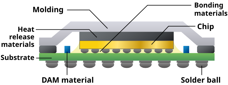
With semiconductor devices featuring higher performance and larger sizes, they also generate technical issues such as warpage and heat. We provide products such as plastic microparticle products that feature excellent gap control by being added to adhesive and joining materials, and high heat dissipation sheets that feature appropriate resilience and deformability by densely filling and orienting carbon fibers into silicon resin.
… Sustainability Products
| Material Category |
Product | Feature | |
|---|---|---|---|
| Microsphere・Filler | Plastic-based Micropearl™ | Plastic particles with uniform particle size distribution. High-performance filler combines properties such as stability, flexibility, and resilience. Can be used as in-plane spacers, stress relaxation materials, and unevenness-forming materials. | Product Information |
| Microsphere・Filler | Metal-plated Micropearl™ | By adding different metal coatings to plastic particles that are the same size, they can work as strong conductive fillers. Our unique manufacturing technology also allows for hardness control. They also act as unique, high-performance lightweight fillers. They have low specific gravity, high dispersion, low resistance, and high flexibility. | Product Information |
| Removable UV Tape | Single-sided Heat Resistance UV Tape [SELFA™ HS] |
UV release tape that combines resistance to various semiconductor manufacturing processes with low residue. Protects device surfaces and suppresses warpage in various PKG manufacturing processes. | Product Information |
| Removable UV Tape | Double-sided Heat Resistance UV Tape [SELFA™ HW] |
UV release tape that combines resistance to various semiconductor manufacturing processes with low residue. Glass support system maintains device flatness during the process and ensures safe handling. | Product Information |
| Removable UV Tape | Single-sided Chemical-resistant Self-releasable UV Tape [SELFA™ MP] |
UV release tape that combines strong chemical resistance and low residue; UV irradiation causes gas generation, which reduces device damage and allows easy peeling. | Product Information |
| Heat Release Related Products | Super Thermal-Conductive Pads [MANION™ Series] |
A heat conductive sheet achieves both flexibility and adhesion by the high thermal conductivity of carbon fiber which uses magnetic field orientation technology. | Product Information |
Related words
BG
BG is an abbreviation of back grind. It is in the late-stage processes of semiconductor production and is a process that grinds a wafer thinly from its backside after circuit patterns have been formed on the wafer surface in the early-stage processes. BG tape used in this process is an essential material, and not only tape but wax and adhesive are also used. Recently, many features such as heat and chemical resistance are required for BG tape as the semiconductor processes have become increasingly complex.
Related Products:UV Releasing Tape [SELFA™]
BGA
A type of IC chip packaging method. The electrodes pins do not protrude around the package, making it ideal for product miniaturization. It uses a grid layout for the external connection terminals on the ball-shaped terminals, with solder balls used for the ball-shaped terminals. The pin-type version is called PGA (Pin Grid Array).
BU Film
BU film is used as an insulating material for semiconductor package substrates that connect semiconductor chips to motherboards and is used for forming fine wiring. As electronic devices require finer wiring and faster communication, this film needs to minimize transmission loss. Additionally, as devices become thinner, it also needs to prevent the warping of the thinned substrates.
Related Products:Build-up Dielectric Film for FC-BGA Substrates NX04 Series (NX04H), NQ07 Series (NQ07XP)
Dam-fill
An insulating material used to form sharp dams on substrate islands for chip mounting or around the periphery of mounted CSP/BGA packages. Its purpose is to control the flow of die attach paste during chip bonding and manage the filling area for underfill. This material has excellent moldability and is a high-reliability solution for reducing package warpage.
Related Products:High-viscosity inkjet ink
Dicing
Dicing is an important and essential process in the late-stage processes of semiconductor production. It is a process that cuts a wafer—on which circuits have been formed—and separates it into individual chips. Dicing methods include blade, laser, and plasma dicing. Blade dicing is widely used, but laser or plasma dicing is sometimes chosen to reduce mechanical damage to the chips, to accommodate very small chips, and in consideration for the environment.
Related Products:UV Releasing Tape [SELFA™]
Dry Etching
Dry etching is a method that removes unnecessary parts physically or chemically using ions in plasma or using reactive gas in a dry way. Generally, dry etching often refers to reactive ion etching, or RIE. Since dry etching allows highly precise shape control and does not require waste liquid treatment, it is used in many production processes.
Fan Out
Fan-out packaging refers to wiring on a larger area than the silicon chip. Fan-out wafer-level packaging (FOWLP), which uses this technology, allows high density wiring while minimizing package thickness by placing many I/O pins in a space around the chip on a redistribution layer (RDL) instead of a conventional plastic substrate to feature higher performance and a thinner shape. In addition, its structure allows multiple silicon chips to be placed.
Related Products:UV Releasing Tape [SELFA™]
FC-BGA
FC-BGA is a high-density semiconductor package substrate for high-speed LSI (Large Scale Integration) devices that uses ball-shaped terminals known as bumps to attach and encapsulate a chip on an ultra-thin substrate. It offers fast data processing capabilities and excellent heat dissipation, and is commonly used in computers, servers, and networking equipment.
Related Products:Build-up Dielectric Film for FC-BGA Substrates NX04 Series (NX04H), NQ07 Series (NQ07XP)
Filler
A filler is a material that is used to fill in space or cavity, referring to small particles or powders added to materials. By compounding fillers with various functions, such as thermal and electrical conductivity, into resins, the filler-composite materials surpasses the functionality of the resin alone. The materials are used in a wide range of applications, from smartphone to airplanes, for their heat resistance and high strength.
Related Products:Heat Release Related Products
Flux
Flux is a chemical agent used for the soldering process in semiconductor production. It removes oxides and foreign substances on metal surfaces to improve solder wettability. Due to the increasing need for reducing processes in recent years, high performance flux materials are also attracting attention.
FPC
A substrate in which conductive metals such as copper foil are laminated to a base film like polyimide to form electrical circuits. It is also called as a "Flexible Printed Circuit (FPC) board," it is extremely thin and lightweight. Unlike rigid substrates, it is also highly flexible and bendable, making it suitable for use in bending parts, three-dimensional configurations, and slight gaps in electronic equipment. With an increasing demand for smaller, lighter, and thinner devices, FPCs are used in a wide range of electronic devices such as smartphones and LCD televisions.
GWSS
Glass Wafer Support System (GWSS) is a temporary bonding and debonding (TBDB) material proposed by SEKISUI CHEMICAL to solve issues such as cracking and chipping of ultrathin semiconductors when transported and warpage of ultrathin wafers. The removable UV tape SELFA™—which releases itself by UV irradiation and developed by SEKISUI CHEMICAL—is used to realize GWSS. For leading-edge semiconductors where the TBDB application is in great demand, research and development efforts are being made continuously to further improve performance such as heat and chemical resistance.
Related Products:UV Releasing Tape [SELFA™]
HBM
High Bandwidth Memory (HBM) is a memory standard defined by JEDEC that uses Through-Silicon Via (TSV) technology for die stacking. HBM is a type of DRAM (Dynamic Random Access Memory) designed to transfer large amounts of data at once, offering 10 to 100 times the data transfer speed compared to traditional DRAM used in PCs. It is utilized in applications such as GPUs (Graphics Processing Units), HPC (High-Performance Computing), and AI (Artificial Intelligence) for tasks like image processing and machine learning due to its high data transfer rates.
Related Products:UV Releasing Tape [SELFA™]
Molding
Molding is a semiconductor process that uses materials such as thermosetting resin to enclose chips after the bonding process to protect the chips from the effects of factors such as external impact, temperature changes, and humidity. There are two types of molding: transfer molding that injects and feeds resin, and compression molding that dips an object into melted resin to shape it.
PoP
Package on Package (PoP) is an assembling method that stacks a semiconductor package on another semiconductor package. This is a technology that allows higher performance and smaller/thinner shapes by stacking semiconductor packages to make full use of the limited space. This technology is rapidly evolving recently as it provides another advantage of faster operation by allowing two packages exchanging data to be closely placed. It is mainly used for mobile devices and consumer electronics.
TIM
TIM (Thermal Interface Material) is a type of thermal conductive material designed to efficiently transfer heat from electronic devices to cooling systems. By providing effective thermal management, TIM ensures that semiconductor devices operate reliably and perform optimally.
Related Products:Heat Release Related Products
TSV
Through-silicon via (TSV) is an electrode made of a through via filled with copper and is formed on silicon interposers and semiconductor chips. With the TSV structure, chips can be stacked to minimize the mounting footprint and wiring and reduce their sizes, increase performance, and save power.
Related Products:UV Releasing Tape [SELFA™]
Underfill
A liquid thermoset resin used for encapsulating integrated circuits. It acts as an adhesive to protect solder joints, which connect electronic components to printed circuit boards, from cracking due to impacts or heat. Underfill is required to have properties such as impact resistance and reworkability.
Related Products:High-viscosity inkjet ink
Wafer
A wafer is a material used in semiconductor device manufacturing. It is a disk-shaped substrate made by thinly slicing a cylindrical ingot made of a material such as highly controlled, single-crystal silicon.
