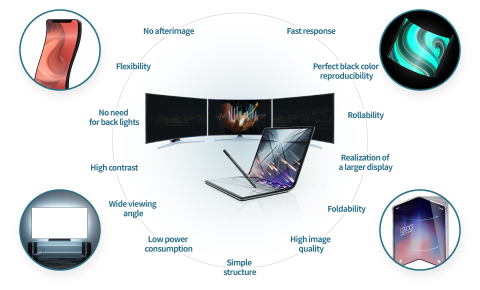
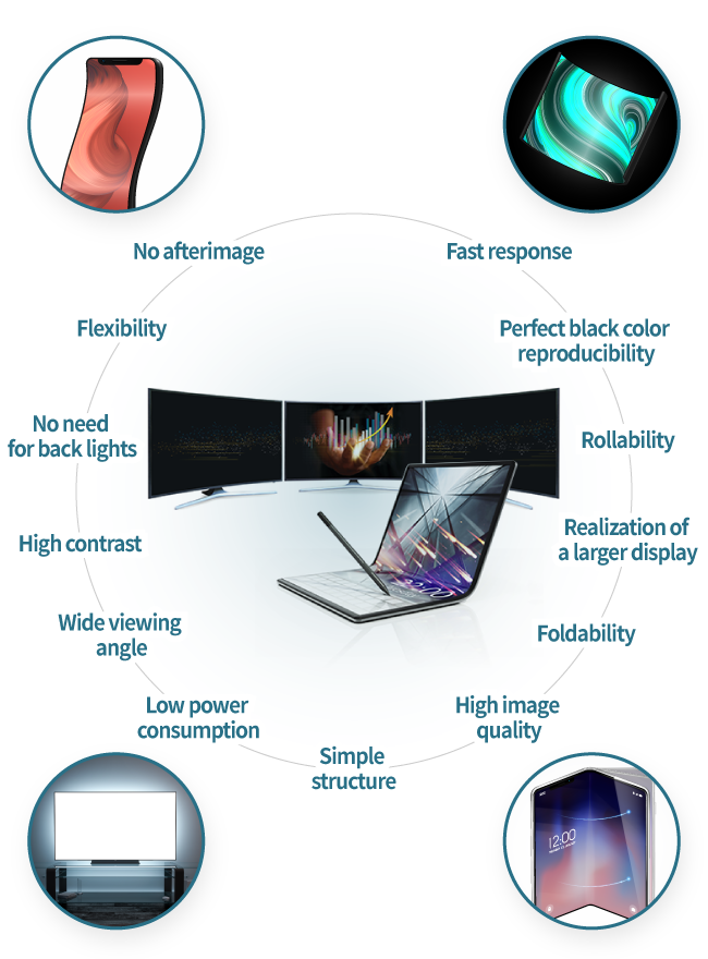
Next-generation display
Continuously evolving display with higher image quality and performance
Sekisui Chemical Electronics materials will contribute to solving issues that arise with this evolution
Shift from LCD displays to OLED displays
- What is an organic EL display (OLED) ?
-
・Organic Light Emitting Diode
OLED displays emit light when a voltage is applied to the organic elements themselves.This eliminates the need for light sources (backlights) such as fluorescent lights and LEDs, which makes OLED displays thinner. OLEDs, which have been used primarily in LCDs, are expanding to use in smartphones.
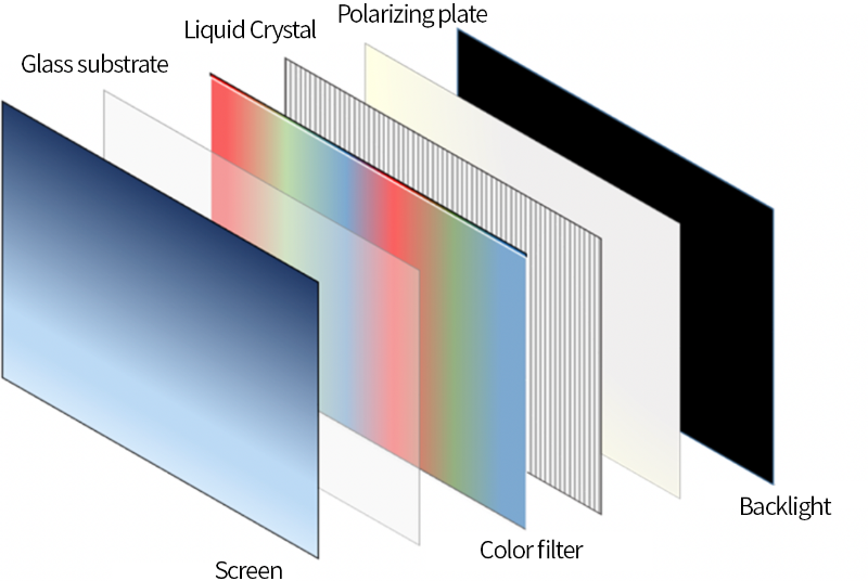
- What is LCD ?
- LCD stands for "Liquid Crystal Display. A liquid crystal is a state of matter between solid and liquid.LCDs have a liquid crystal layer sandwiched between two glass substrates, whose property makes it possible to control light and project images. Liquid crystal substances themselves do not emit light. Therefore, images are projected on LED displays by controlling light sources (backlights) such as fluorescent lights and LEDs.
Features of OLED
What is so great about OLEDs ?
The main difference is that OLEDs are lighter and thinner than LCDs. In addition, organic EL elements themselves emit light, which allows for perfect black levels. One remarkable feature is excellent flexibility. Its flexibility allows for the installation of curved displays on foldable smartphones and commercial digital signage. And, with this flexibility, products can be differentiated from others.
What are the issues of OLEDs?
The advantages of OLEDs are not used effectively.
Though OLEDs have many advantages, most of them are not being used. It is said that they are able to consume less power than LCDs in principle. However, this has not yet been achieved with current OLEDs. And, though the structure of OLEDs is simpler than that of LCDs, the manufacturing process is more complex. Therefore, process and cost reductions need to be solved with a variety of materials.
Issues of fordable smartphones
Their main feature is that they are foldable, however, opening and closing them can easily cause cracking in some materials. Development of higher-quality foldable smartphones is currently underway, solving issues such as preventing occurrence of creases and cracks.
Characteristics of Sekisui Chemical's products that address problem-solving
Excellent functionality
- Moisture permeability, Repulsion resistance, Durability
- Water resistance, Dust resistance, Flexibility
- Heat resistance, Shock resistance, High insulation resistance
- Great transparency, Low moisture permeability, Low dielectric property
High performance processes
- Going into B stage, Moisture curing, UV curing
- Customization, Process reduction, Molding technology
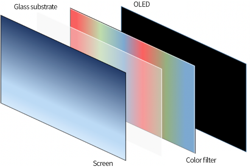
Structure of OLED
Coloring methods of OLED
RGB coloring method
A single pixel consists of red, green, and blue, each of which emits light independently. With no filters to block light, high luminous efficiency and high luminance can be achieved.
Color filter method
Colors are produced through a combination of OLED elements that emit white light and RBG (red, blue, and green) color filters.OLEDs produce greater black levels with higher contrast ratio than LCDs. However, compared with the RGB coloring method, luminance and luminous efficiency become lower, with high power consumption.
OLED light extraction method
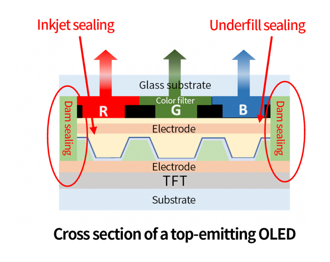
- Top emission method
-
- The light emission occurs in an upward direction against the TFT substrate.
- A high aperture ratio is achieved because light is not blocked by the TFT substrate. Bright and high-definition.
- Low power consumption.
- Difficult to develop.
- Bottom emission method
-
- The light emission occurs in an downward direction against the TFT substrate.
- The color filter is obstructed by circuits of the TFT substrates and others, resulting in a low aperture ratio and darker color.
- Increasing brightness causes higher power consumption.
- Easy to develop and manufacture.
There are two methods to extract light from OLEDs: top emission and bottom emission. Although each method has its own issues, more and more manufacturers are adopting the top emission method as a cutting-edge technology to achieve high luminance and resolution.
OLED models
Rigid OLED
A rigid OLED is produced by the vacuum deposition method with a TFT circuit and OLED layers on glass substrates. An optical fingerprint sensor can be mounted.One of the advantages is that stable production is possible at low cost.
Flexible OLED
PI (polymide) is coated on a flexible substrate such as a plastic one. A TFT circuit and OLED layers are then formed on it. Finally, the PI film is peeled off to create a flexible OLED. It is very flexible and bendable, which makes OLED displays thinner and lighter.In addition, since there is no air layer, not only an optical fingerprint sensor but also an ultrasonic fingerprint sensor can be mounted.
Technical issues of flexible OLEDs
- Organic EL is sensitive to water.
-
Organic El elements are not tolerant of water, so it is necessary to prevent them from exposure to moisture.The moisture seal process is important for a long product life cycle.
In the top emission method, advanced sealing technology is required.
Sekisui Chemical's sealing technology
- UV delayed curing type
- Full curing at low temperature
- Excellent low moisture permeability
- Low outgas
Go to higher-performance displays
Structure of an OLED smartphone
Flexible smartphones
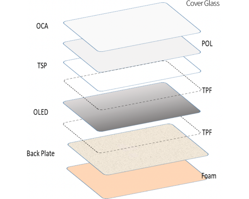
In the production processes of flexible smartphones, various materials such as glass and acrylic need to be laminated together.
Various laminating and mounting materials for OLED applications are available in the Sekisui Chemical Electronics Field.
Foldable/Rollable smartphones
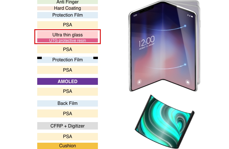
- Switching from PI to UTG
-
A weak point of PI and PET layers is poor flexural properties.
Repeated bending produces streaks.Using UTG can produce fewer creases and give off a sense of high quality peculiar to a glass.
- UTG also has its own problem
-
UTG cracks more easily than plastics such as PI substrates.
With our UTG protective resin applied, UTG can be made less susceptible to cracking.
Sekisui Chemical's thin-film cushioning material
with excellent shock absorption
and flexibility <XLIM>
What is XLIM?
XLIM is an ultra-thin, high-performance foam that combines superior functionality and reliability, and is the industry's thinnest at 0.06 mm. It can contribute to improved design and functionality in cutting-edge devices such as smartphones.
Features
- ・Shock resistance
- ・Improved sound directivity
- ・High sealing properties
- ・Chemical resistance
Applications
- ・Display protection
- ・Various water-proof materials
- ・Module gaskets for LCDs and OLEDs
Sekisui Chemical's UTG protective resin
- Shock resistance※1
- Great bendability
- Prevention of glass shattering
- Excellent transparency
※1 Pen drop test
Larger OLEDs
Organic EL (OLED) TV
One of the remarkable features of OLED TVs is that each element is self-emitting, so they do not require a backlight or a liquid crystal layer as LCD TVs do. This enables OLED TVs to be thinner or lighter. TV sets are becoming large and larger. However, while there are advantages in various methods, there are also issues such as cost, contrast, and the complexity of the manufacturing processes.
- LCD TV
-
- Organic EL (OLED) TV
-
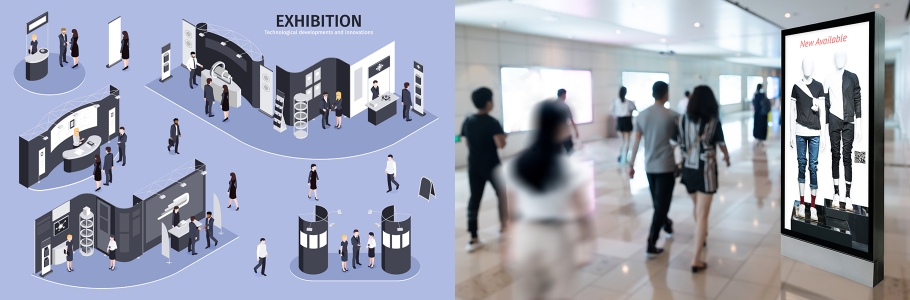
Digital signage
OLED displays take advantage of their light weight, thinness, and flexibility to enable curved surface displays, which are used in commercial digital signage applications.They can be installed in various facilities, regardless of location, and can display a variety of images and text.
Sekisui Chemical's electronics related products
A lineup of exterior materials for use around display housings is available.
- Foam tape
- Adhesive tape
- Molded products
Next generation key technology following OLED
miniLED
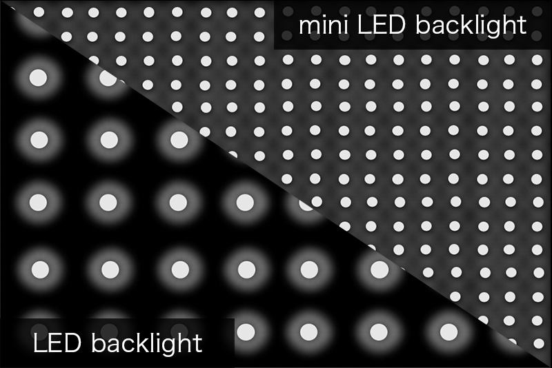
- Usable for small portable device applications for TVs, PCs, tablets, and smartphones
- By dividing the backlight, light leakage, a weak point of ordinary liquid crystal panels (LCDs), is controlled, resulting in improved brightness, contrast ration, and reproduction of blacks.It is now being used not only in small and large TVs, but also in small and medium-sized devices such as tablets.
microOLED
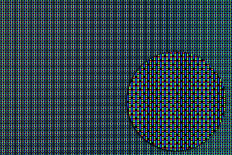
- Usable for small devices such as smart glasses, small camera viewfinders, and projectors
- Smaller OLED displays.Light-emitting layers of an OLED can be formed on a silicon wafer, not a glass substrate. Pixel size is less than 10μm, realizing high resolution in a small size while maintain the features of OLEDs. The latest micro displays with features such as high-definition and high-speed response.
microLED
- It is expected to be put to practical use in wearable devices such as eyeglass-type wearable devices.
- Micro LED display
This is a display in which each LED (Light Emitting Diode) consists of one pixel.Since each LED emits light as a pixel, color reproducibility is high, and response time is fast, equivalent to that of an organic light-emitting diode (OLED) and 100 times faster than that of a liquid crystal display (LCD).It does not have the problems of OLEDs, such as short lifespan and burn-in, and can be used for curved surface displays. There are many issues at present, and mounting ultra-small LED chips on substrates requires sophisticated technology and yield improvements. In addition, μLED requires a number of LEDs corresponding the number of pixels, resulting in high manufacturing costs.
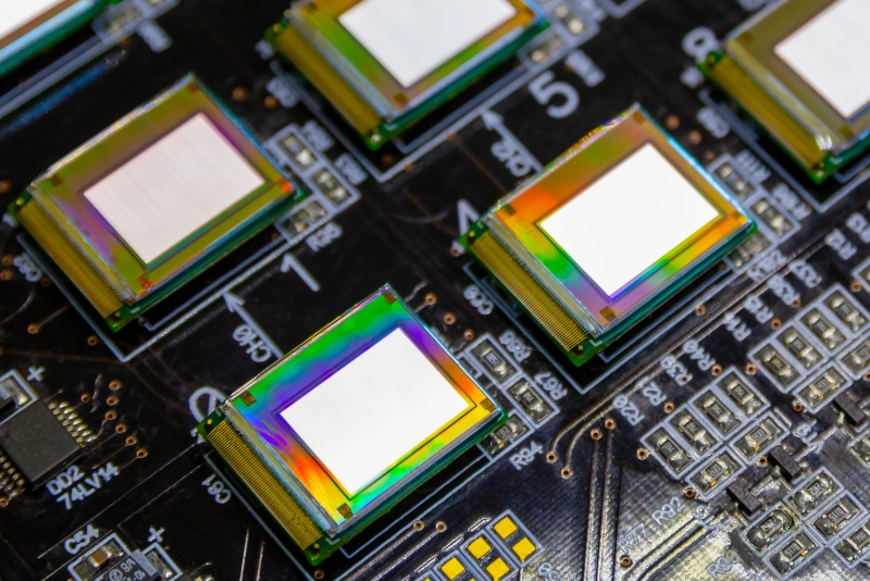
Sekisui Chemical's development toward addressing new LED and OLED technology issues
Inkjet materials/Sealing materials/Connectors
In the Sekisui Chemical's electronics field, we are working on various developments as next-generation displays evolve.
We continue to make contributions by developing new displays and manufacturing many materials such as tapes, foam products, mounting materials, and heat dissipation-related products for AR/VR applications and will provide high-quality product technologies.